Recreating the Iskra Delta Partner Motherboard

In 2023, I completed a project that, at the start, seemed unlikely to succeed. I built an Iskra Delta Partner motherboard from scratch. I did not repair an old one. I recreated the entire thing, beginning with a damaged and unusable board and ending with a working machine.
This was not an engineering exercise. I have no real background in electronics. What I had was a broken board, enough tools, and a process that I believed could work.
Step 1: Strip the Board
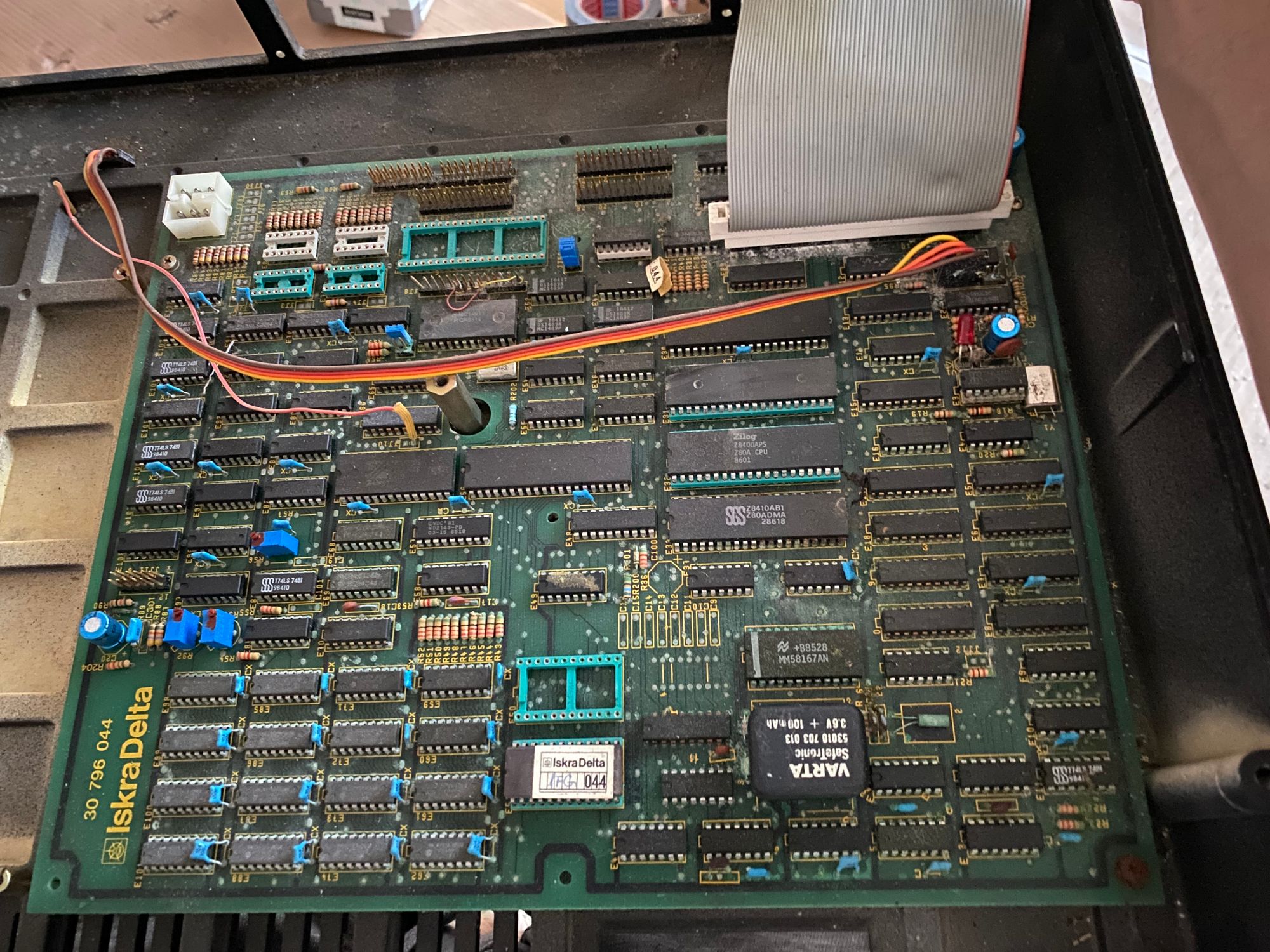
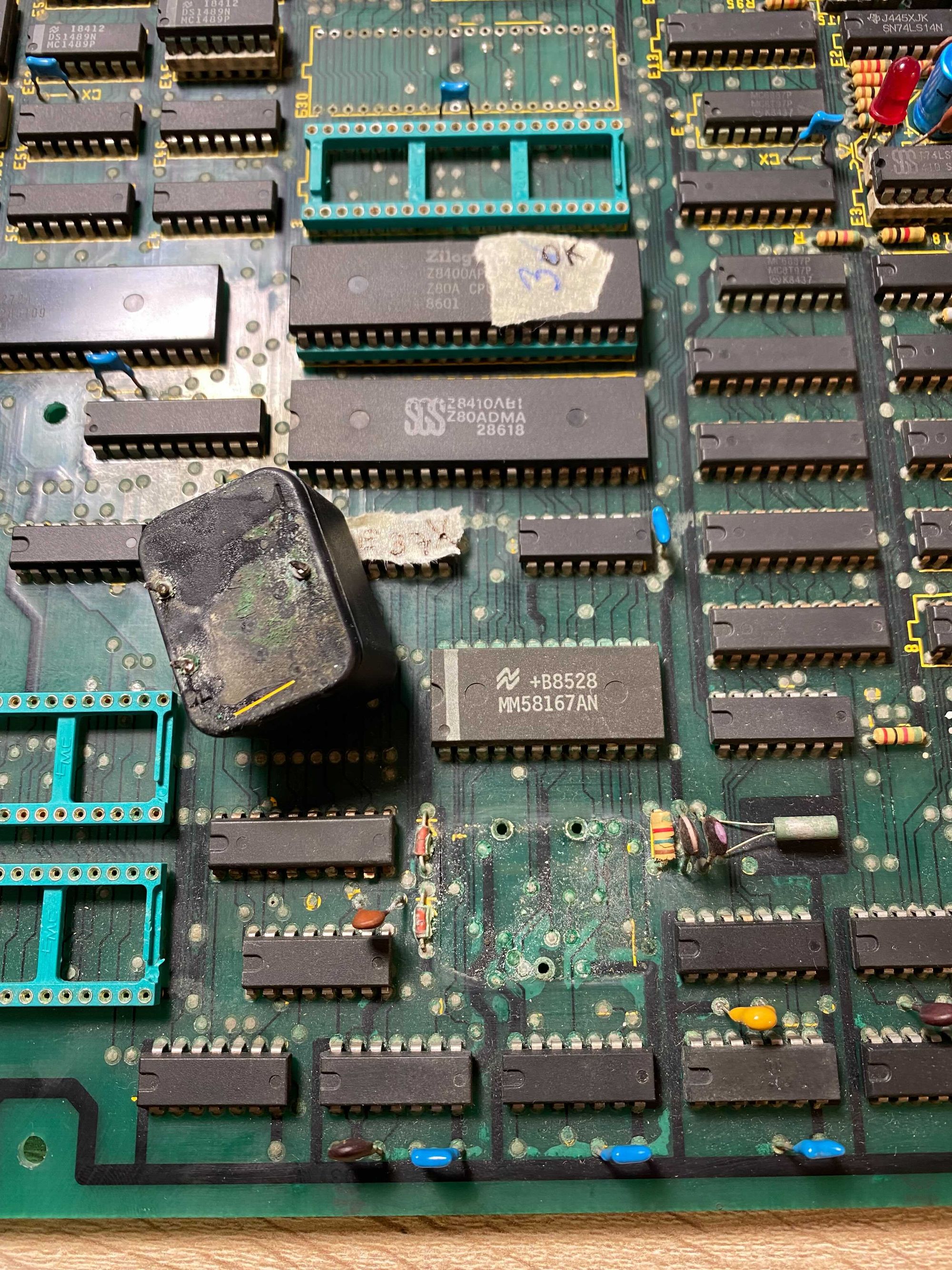
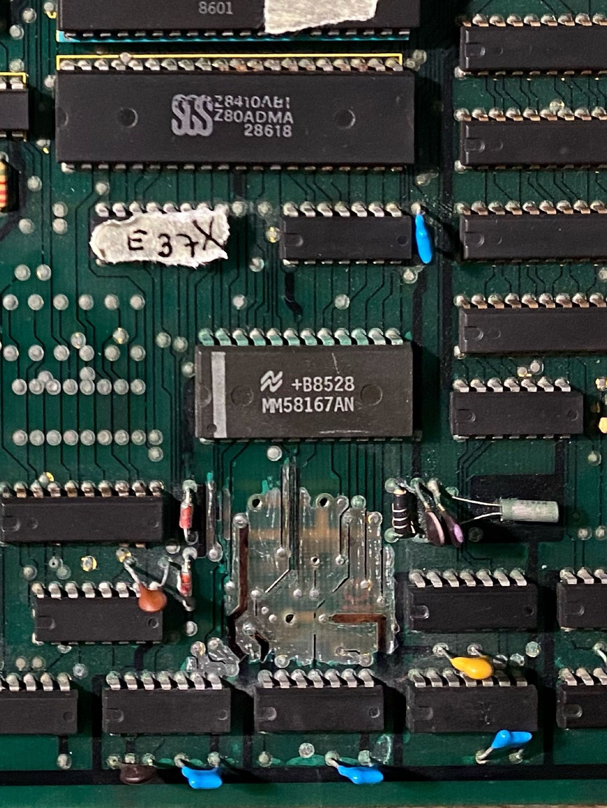
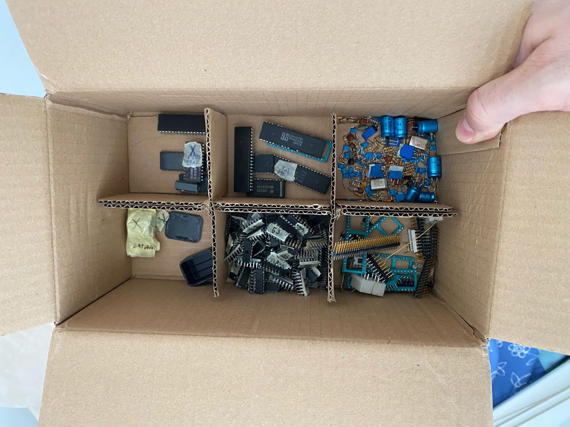
The original board was badly oxidized. I suspect this was the result of both battery leakage and moisture exposure. The damage was severe, and although I cannot say for certain that none of the components were usable, that felt like a fair assumption.
Desoldering oxidized joints turned out to be more difficult than I expected. The oxide layer blocked heat, so the solder would not melt. After trying several approaches, I found the most reliable method was to cut the joint from underneath, exposing clean solder. Once that was exposed, I could melt it and use a desoldering gun to remove the component. It was a slow process, and it took patience.
In the end, I was left with a bare board. The components were gone, but the layout was still visible.
Step 2: Scan the Board
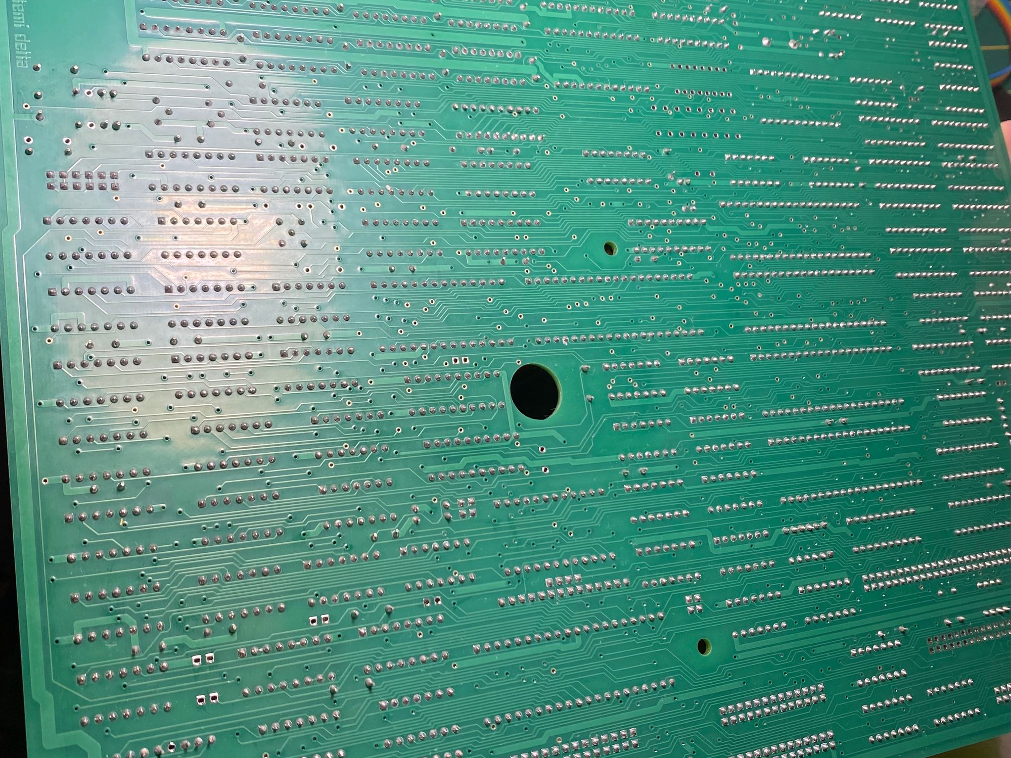
Fortunately, the Partner board has only two layers. I scanned both sides at high resolution. The scans gave me a clear reference for every trace, pad, and via. That was enough to begin recreating the design.
Step 3: Redraw in KiCad
I used KiCad to build a new version of the board. To identify and place the vias, I created a tool specifically for this task. It used older AI technologies such as vector spaces and similarity measures. I have written about that process elsewhere.
Once the vias were in place, I manually added all the components and drew every trace on both layers. It was time-consuming but straightforward. I was not working from a schematic or simulation. I was just copying what I saw in the scan.
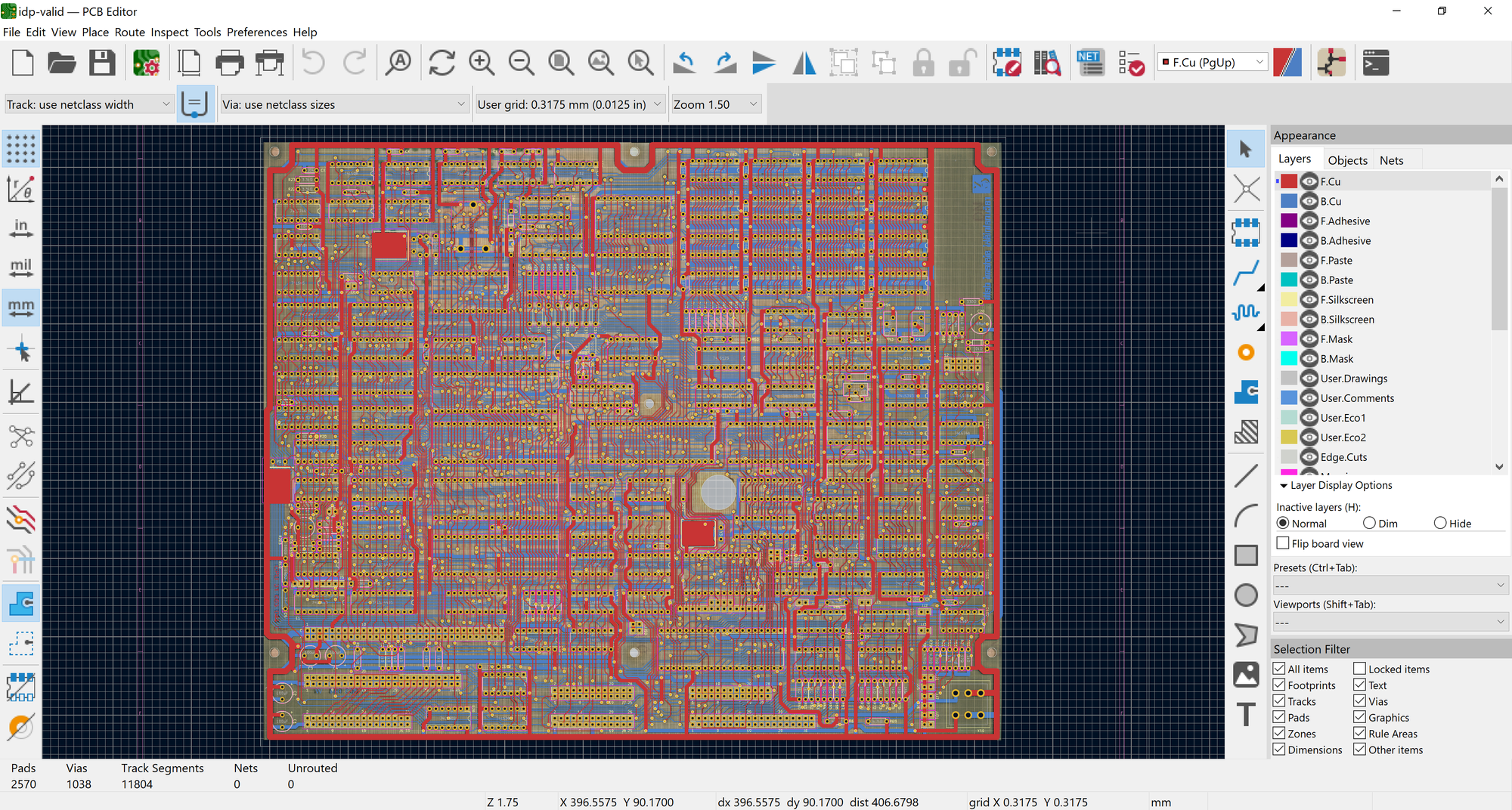
Step 4: Validate the Layout
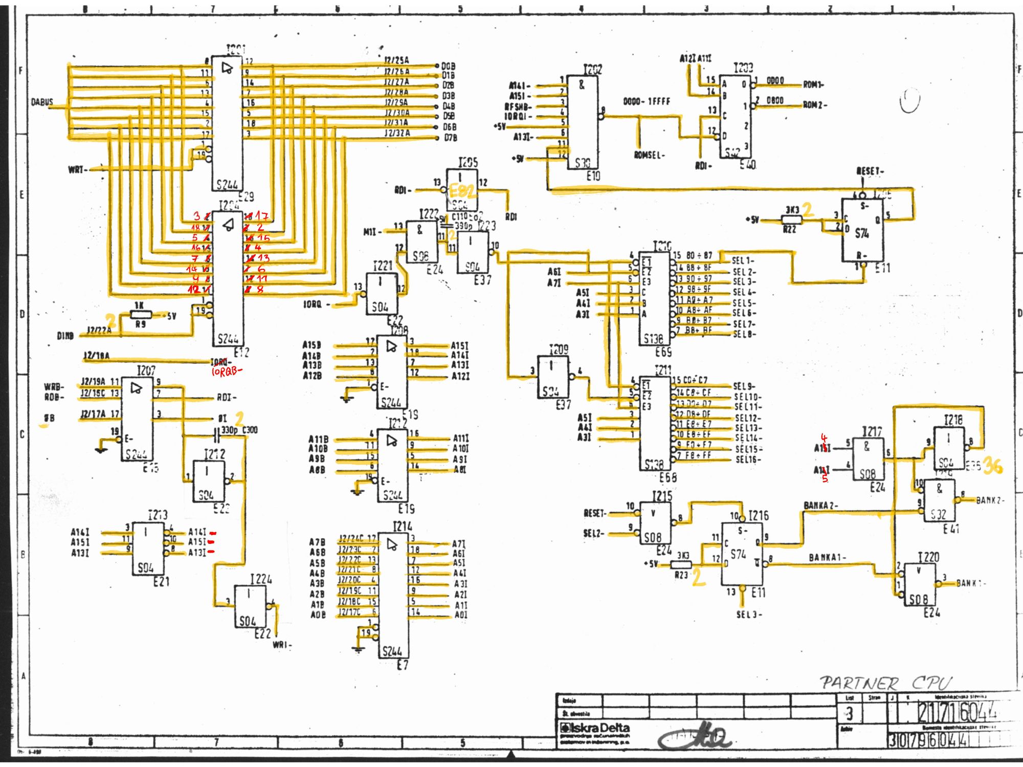
To make sure the KiCad layout matched the original design, I needed a second source of information. I had access to the original schematics, but they were not entirely reliable. Some were poorly scanned, and others contained mistakes. I could not depend on them completely.
Still, they were useful for cross-checking. My friend Sašo and I transcribed all the network connections from the schematics into a text file. I also wrote a Python program to extract the network data from the KiCad layout using a flood fill algorithm.
I then compared the two sets of data. Whenever there was a mismatch, it was usually obvious whether the problem was in the schematic or in my layout. I fixed the layout or adjusted the network list until both matched exactly.
That process took longer than expected, but once it was complete, I was confident that the recreated layout was accurate.
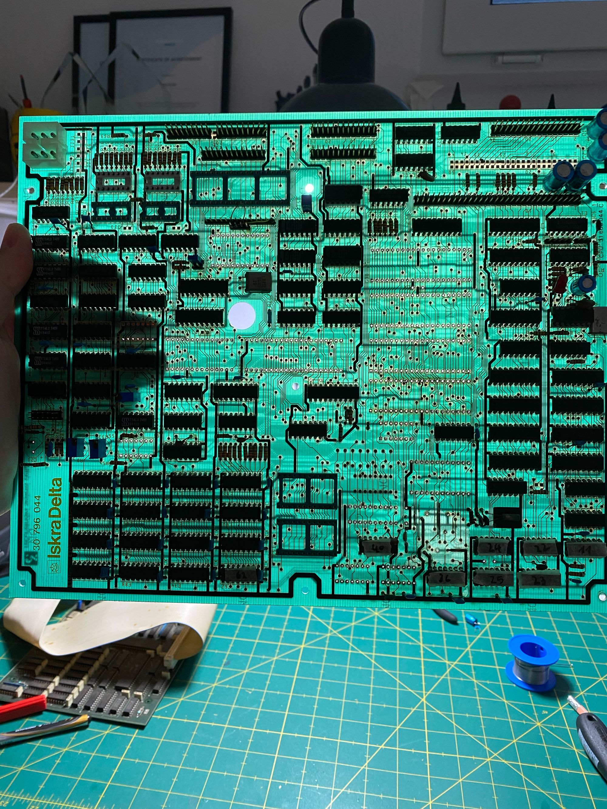
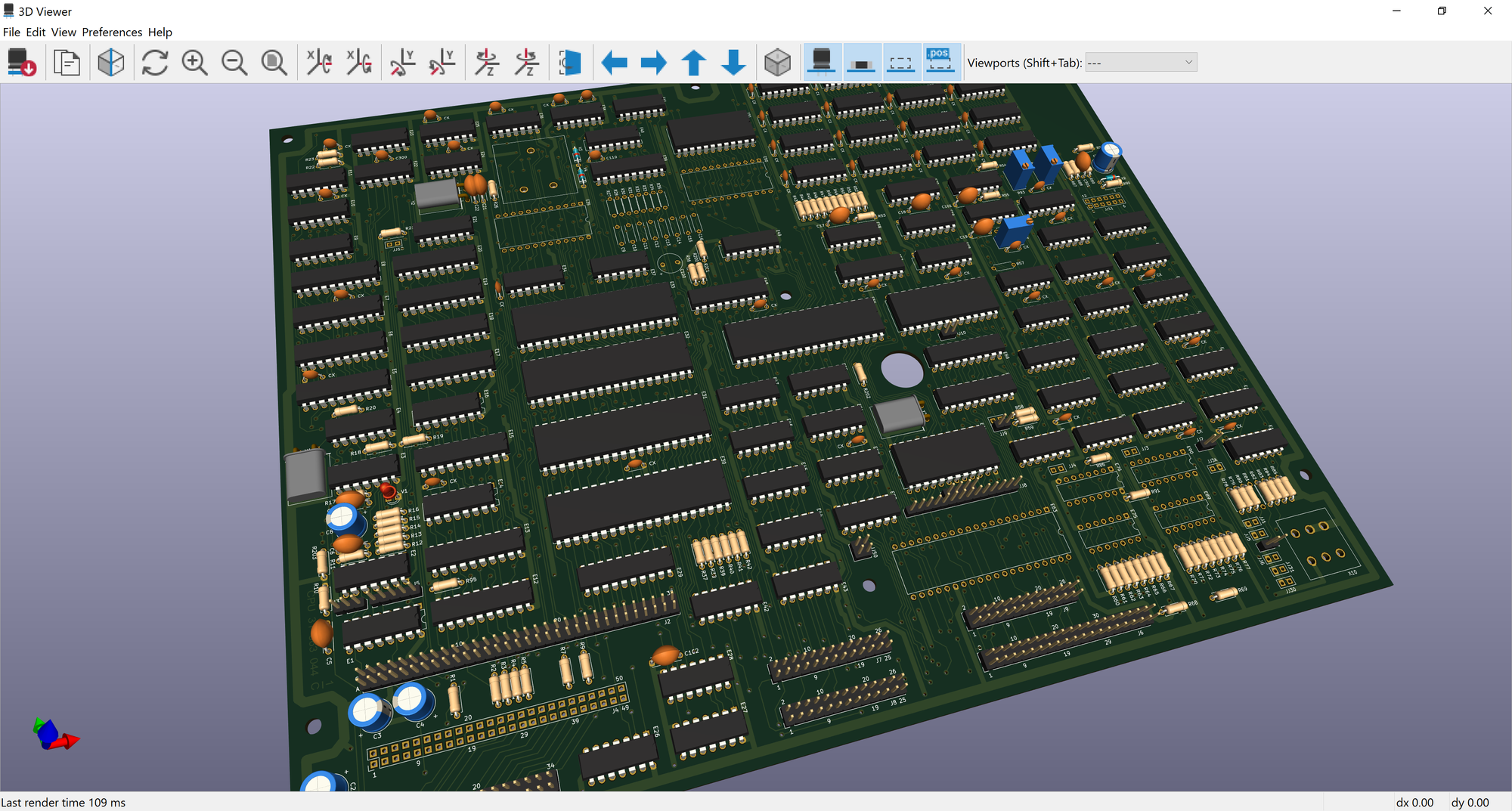
Step 5: Manufacture the Board
With validation complete, I exported the board as Gerber files and sent them to PCBWay.
The boards came back looking perfect. The fabrication quality was excellent. It was the first time in the project where I felt like something solid had been created.
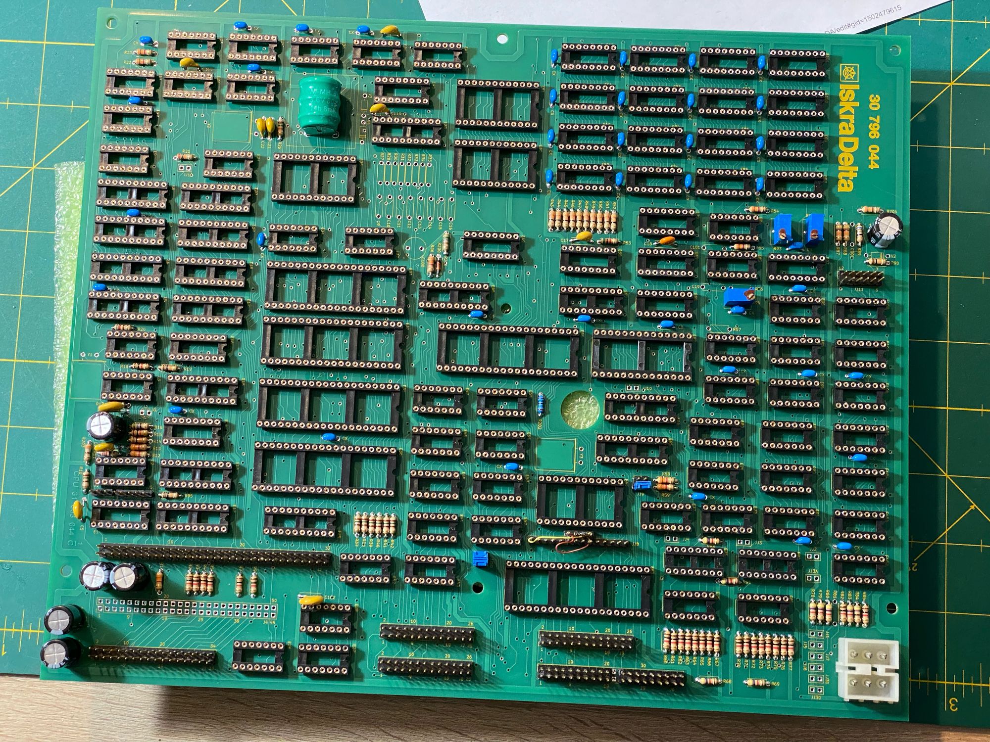
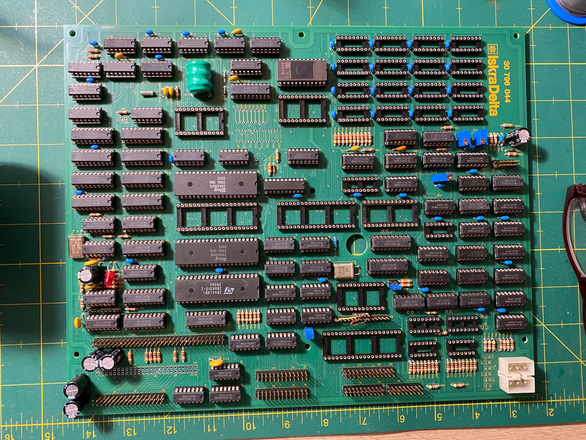
Step 6: Assembly
I assembled the board using components from several sources. Most came from Mouser. A few came from stores here in Slovenia. Some I bought on eBay. Others were donated by members of the local retro computing community.
The process of soldering everything into place was uneventful. The board was well laid out, and with the components correctly sourced, there was nothing unusual.
Step 7: Switching It On
The board worked on the first try.
That outcome might sound simple, but it was the result of many careful steps. The work had not been fast or elegant. But it had been systematic, and each stage had been checked before moving on. So when the moment came to power it up, it worked.
Why I Did It
This was not a technical achievement. I started the project without knowing much about electronics, and I finished it in roughly the same state. But that was never the point.
I wanted to see if it was possible to rebuild the board by treating the damaged original as a kind of visual map. I trusted the process and was willing to do the manual work. That turned out to be enough.
There are many ways to experience retro computing. Most are easier than this. But this approach created something unusual. It was not an attempt to learn the system. It was just a decision to rebuild it, step by step, without skipping anything. And it worked.